Explain briefly the VSB-SC modulation
Generation of VSB signal:
The block diagram for generation of VSB signal is shown in Fig. 17. The block diagram consists of incoming message signal \(x\left(t\right)\), carrier signal \(A_ccos2\pi f_ct\), balanced modulator and a Low Pass Filter (LPF). First of all a DSB-SC signal is generated by balanced modulator where two incoming signals message and carrier signal are modulated in the balanced modulator. The modulated DSB-SC signal is applied to the LPF and VSB-SC signal is generated.
Let us consider the transfer function of LPF is \(H\left(f\right)\), the expression of VSB signal can be defined in frequency domain as
\(S\left(f\right)=\frac{A_c}{2}\left[X\left(f-f_c\right)+X\left(f+f_c\right)\right]H\left(f\right)\)
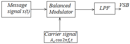
Fig. 17.Block diagram of generation VSB signal
According to the Fig. 18, the bandwidth of the VSB signal is \(\left(f_c+f_m-f_b\right)\) unit. Here the area of the lower side band and upper side band spectrum of the VSB-SC spectrum are not same. Some information can be losses in the upper sideband (defined as dotted line) and it should be compensated by the lower sideband area. The bandwidth of DSB-SC signal and SSB-SC signal are \({2f}_m\) and \(f_m\) whereas for VSB signal \(\left(f_c+f_m-f_b\right)\). Therefore considering bandwidth we can write \(\left(DSB-SC<VSB<SSB-SC\right)\) and \(f_m>f_b\)
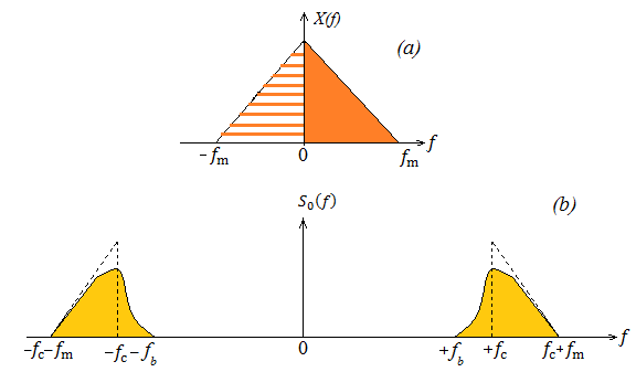
Fig. 18(a) Spectrum of message signal and (b) Spectrum of VSB-SC signal

What is scattering Parameters? Why is it used in microwave Network?

Write short note on LVDT
State and prove the Parseval’s theorem for power.
What is strip line?


1.png) Fig. 15(a)
Fig. 15(a)