Tunnel diode is specially made p-n junction device which exhibits negative resistance over part of the forward bias characteristics. It has extremely heaving doping on both sides of the junction and an abrupt transition from the p – side to the n- side.
Under unbiased condition, there is just the same probability of electrons going from states in the conduction band on the n side to the states in the valence band on the p- side, as in case of p material.
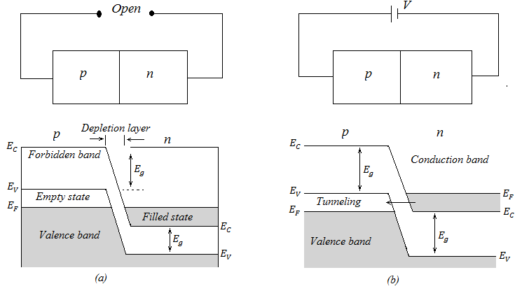
 Fig. 25(a) Tunnel diode under no biased condition and (b) Tunnel diode under forward biased condition
The main criterions for tunneling are
- Fermi level is within the band.
- The barrier of the deletion layer at the junction is very thin (≈100A°) and which can be achieved by means of heavy doping (≈1021 atoms/c.c) in both the p and n layer. Thus the particle have the lower kinetic energy cannot cross the barrier height but have the probability that they can tunnel through the potential barrier.
- At 0 K, all the states above Fermi level are empty and below Fermi level all the states are occupied.
- There must be filled energy states on the side from which particle will tunnel and allowed empty states on the other side into which particle penetrates through at the same energy level.
Fig. 25 shows the energy band diagram of a tunnel diode under no bias and forward biased condition. Initially at zero bias condition as no filled states are available in any side of the junction, hence no tunneling takes place. With the application of forward bias voltage, the conduction band upward and creates vacancy level in the p- side and as a result tunneling takes place.
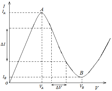
The I-V characteristics of Tunnel diode is given in Fig. 26.
 Fig. 26 I-V characteristic of Tunnel diode.
From the forward characteristics curve we see that with the increase of forward biasing voltage from zero the tunneling current starts to follow from n- side to p- side and reaches the peak value IA. With further increase of forward bias voltage i.e. for V>VA, the conduction band rises further up and as a result no corresponding allowed empty state is available in the p- side, hence no electro can tunnel through the barrier and the tunneling current drops nearly equal to zero as shown by IB and the corresponding voltage VB in the I-V characteristic curve. This valley current results due to the presence of defect states within the semiconductor energy gap. Such a current in the valley region can also be called as the excess current.
When the forward bias voltage V is increased above the valley voltage VB, the ordinary injection current I at the p – n junction starts flow. This injection current increases exponentially in its normal course with the increase of forward biasing voltage.
Total current density in tunnel diode is
J=JTunn+JExces+JTher
Tunneling current density is
JTunn=JA(v/vA)exp(1-V/VA)
Where JA is the peak current density corresponds to peak voltage VA at point A.
Excess current density is
JExces= JBexp[α(V-VB)]
Where JB is the valley current density at point B and α is constant.
The thermal current density is
JTher=JS[exp(qB/nkT)]
Where 1<n<2 and JS is the saturation current density. One of the available empirical curve fitting expressions to represent the complete tunnel diode I-V characteristics is given by
\(I=\frac{(I_A-I_B)}{{(V_B-V_A)}^5}\left[5\left(V-V_A\right)\left(V-V_B\right)^4-\left(V_B-V_A\right)^5\right]+I_B\)
Where VB=Valley voltage at point B
VA=Peak voltage at point A
IA=Peak current at point A
IB=valley current at point B
This equation does not yield I=0 for v=o, unless a specific relation exists between IA/IB and VB/VA. A simpler approximation may be derived on the basis of the fact that between the peak and valley points of the I-V curve of the tunnel diode resembles a sine wave. The empirical relation then follows to be
I=A+Bsin\ (C In V+D)
Where A, B, C and D are arbitrary constants.
