The device that generates an amplitude modulated wave is called an amplitude modulator. In this method, the linear device that will be used is a normal P-N junction diode.
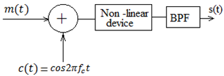 Fig. 34 Model of square law modulator

Fig. 35 Circuit diagram of Square law modulator
The basic block diagram of the square law modulator is given in Fig 34. When a non linear element such as a diode is suitably biased and operated in a restricted portion of its characteristic curve, we find that the transfer characteristics of the diode load resistor combination can be represented closely as a square law. The output of the nonlinear device is given by
\(v_o\left(t\right)=A_1v_i\left(t\right)+A_2{v_i\left(t\right)}^2\) ………………. (1)
Where \(v_i\left(t\right)\) and \(v_o\left(t\right)\) are the input and output signal of the circuit respectively, shown in Fig 35. \(A_1\) and \(A_2\) are constant. The input of the non linear device is
\(v_i\left(t\right)=c\left(t\right)+x\left(t\right)\)
\(v_i\left(t\right)=A_ccos2\pi f_ct+x\left(t\right)\)………….. (2)
Where c\left(t\right) and \(x\left(t\right)\) are carrier and base band signal. Therefore substituting equation (1) in equation (2), we have
\(v_o\left(t\right)=A_1\left(A_ccos2\pi f_ct+x\left(t\right)\right)+A_2\left(A_ccos2\pi f_ct+x\left(t\right)\right)^2\)
\(v_o\left(t\right)=A_1A_ccos2\pi f_ct+A_1x\left(t\right)+A_2{A_c}^2{cos}^22\pi f_ct+2A_2A_cx\left(t\right)cos2\pi f_ct+A_2{x\left(t\right)}^2\)
\(v_o\left(t\right)=A_1A_c\left(1+2\frac{A_2}{A_1}x\left(t\right)\right)cos2\pi f_ct+A_1x\left(t\right)+A_2{x\left(t\right)}^2+A_2{A_c}^2{cos}^22\pi f_ct\) ……. (3)
The first term of equation (3) is the amplitude modulated wave with modulation index \(m_a=2\frac{A_2}{A_1}\). The remaining three terms are unwanted and can be removed by filtering.
\(v_o\left(t\right)=A_1A_c\left(1+2\frac{A_2}{A_1}x\left(t\right)\right)cos2\pi f_ct+A_1x\left(t\right)+A_2{x\left(t\right)}^2+\frac{A_2{A_c}^2}{2}\left(1+cos4\pi f_ct\right)\) …… (4)
Now taking Fourier Transform on both side of equation (4), we have
\(\(V_o\left(f\right)=\frac{A_1A_c}{2}\left(\delta\left(f-f_c\right)+\delta\left(f+f_c\right)\right)+A_2A_c\left(X\left(f-f_c\right)+A_2A_cX\left(f+f_c\right)\right)\)$$+A_1X\left(f\right) +A_2X\left(f\right)\ast X\left(f\right)+\frac{A_2{A_c}^2}{2}\delta\left(f\right)+\frac{A_2{A_c}^2}{4}\left(\delta\left(f-{2f}_c\right)+\delta\left(f+2f_c\right)\right)$$ ……… (5)
Where, \(\frac{e^{-j\theta}+e^{j\theta}}{2}\) , \(F\left\{\left(t\right)\right\}=X\left(f\right)\) and \(F\left\{v_0\left(t\right)\right\}=V_0\left(f\right)\), \(A_1>A_2\)
Symbol ‘ * ’ is the convolution operator.
1.png) Fig. 36(a) Base band signal in frequency domain.
Fig. 36(a) Base band signal in frequency domain.
Square-law-modulator2.png) Fig. 36(b) Spectrum of \(V_o\left(f\right)\)
Fig. 36(b) Spectrum of \(V_o\left(f\right)\)
The modulated signal \(v_o\left(t\right)\) and modulating signal \(x\left(t\right)\). The modulating signal \(x\left(t\right)\) has been assumed to be band limited in the interval -\(f_m\le f\le f_m\). The unwanted frequency components can be removed by using band pass filter (BPF). It can be seen from Figure 36(b) that since \(X\left(f\right)\ast X\left(f\right)\) is band limited in \(2f_m\), there can be over lapping of the spectra when \(f<3f_m\). Thus in order to avoid spectral overlapping the carrier frequency \(f_c\) must be greater than three times the bandwidth of the frequency signal.
In such a case the desired amplitude modulated wave can be obtained by passing the resultant signal through a BPF of bandwidth \(2f_m\) having the centre frequency \(f_c\).