Write short notes on:
A typical circuit diagram of Ring modulator is given in Figure 10(a). The ring modulator consists of two centre trap transformers T1, T2 and four non-linear devices i.e. p-n junction diodes D1, D2, D3 and D4. Carrier signal c(t) with frequency fc is applied at the center tapes of two transformers. The modulating signal x(t) or message signal is applied at the primary wending of the input transformer T1 and modulated signal (DSB-SC) is obtained from the secondary wending of transformer T2.

Figure 10 circuit diagram of Ring modulator
Working principle of the circuit:
Let us consider all the used p-n junction diodes are made by same material and perfectly matched and it is operated as a perfect switch by ON and OFF. A sinusoidal modulating signal x(t) with maximum frequency fm at the input of the circuit and a square wave carrier signal with frequency fc at the centre taps of two transformers are applied. The applied carrier signals amplitude and frequency is very much higher than the modulation signals amplitude and frequency. The transformers both are perfectly center taps and carrier signal is applied exactly at the center of both the transformers. The DSB – SC signal is generated by this modulator. The waveform of the ring modulator circuit is given in Figure 11. Where (a) is the message signal, (b) is the rectangular carrier pulse signal and (c) is the modulated DSB-SC waveform.
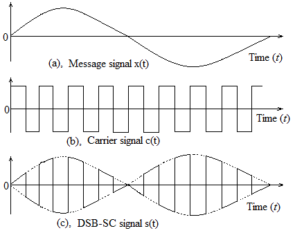
Figure 11 Waveform of the DSB-SC signal of Ring Modulator.
Draw and explain the square – law modulator.
What is Carson’s rule? Explain it.